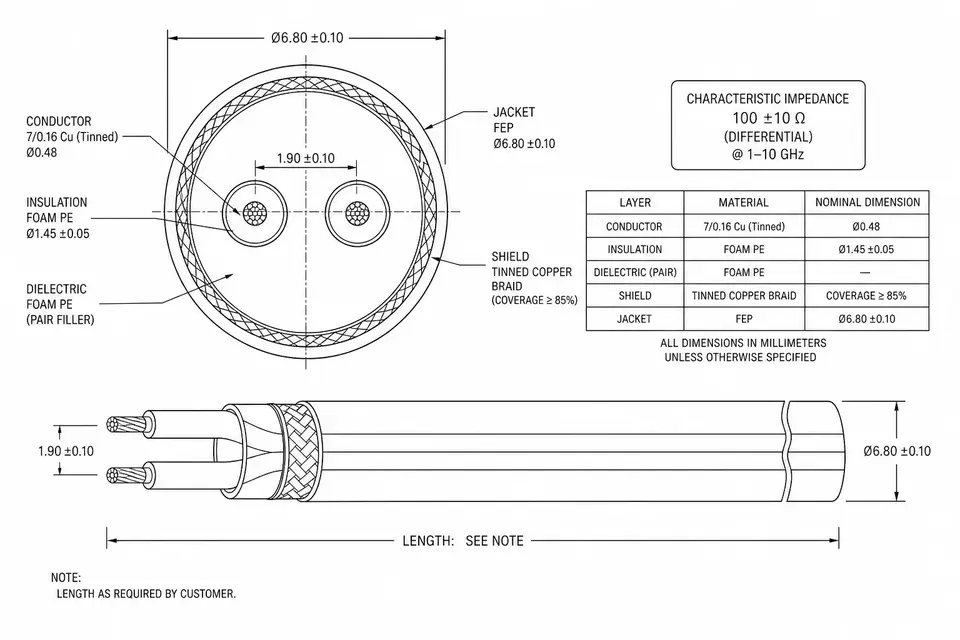
Can You Substitute 90 Ohm and 100 Ohm Cable?
Do not approve the substitution from nominal impedance alone. Read the exact protocol revision and both endpoint specifications, then assess the complete channel against its agreed limits. Neither value is universally better. A tolerance overlap or a cable marked “100Ω” does not establish compatibility with a different interface.
Differential characteristic impedance relates differential voltage and current for a propagating mode. It is not the DC resistance measured with a multimeter. Conductor geometry, dielectric properties, coupling, shields and launches all affect the result. Receiver termination and the reference impedance used to normalize S-parameters are separate quantities.
Record the Controlling Requirement
| Field | Record | Decision |
|---|---|---|
| Interface | Protocol revision and lane mode | Identify the applicable specification |
| Quantity | Differential, common-mode or termination | Compare the same quantity |
| Location | PCB, connector, cable or channel | Mark the controlled section |
| Limits | Nominal value, tolerance and conditions | Resolve conflicting requirements |
| Method | TDR or frequency-domain test | Use the prescribed procedure |
| Coverage | Qualification, process or release | Agree sample count and reporting |
Consult the versioned USB-IF specification library and the exact component data sheets. Do not extend a target from one generation or cable topology to every USB, display or MIPI implementation. If a drawing, endpoint data sheet and procurement specification disagree, obtain a written engineering disposition before release.
A Ten-Ohm Step: What the Calculation Shows
For an ideal lossless line with one abrupt impedance step, Γ = (Z2 − Z1) / (Z2 + Z1). A wave travelling from 90Ω to 100Ω gives Γ = 10/190 ≈ +0.0526; the reverse step gives approximately −0.0526. The reflected voltage amplitude is about 5.26% of the incident amplitude in this simplified model. It is not 5.26% packet loss, a bit-error rate or a measured assembly result.
This application of the Tektronix reflection-coefficient explanation illustrates a single boundary. A real cable has two ends, losses and multiple transitions. Electrical length, edge rate, transition geometry and receiver margin determine how the reflections combine; the calculation cannot decide compliance.
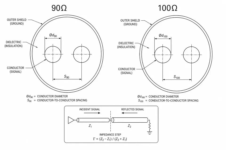
The drawing identifies geometry and an ideal step; it is not a dimensioned construction or test result. Open the complete line drawing.
Six Checks Before Comparing TDR Reports
Map the path: source PCB → launch → mating connectors → cable → mating connectors → sink PCB. A uniform cable section can meet its target while a launch causes a local discontinuity. TDR helps locate changes versus time; S-parameters address frequency-domain behavior such as insertion loss and return loss.
| Check | Evidence to retain | Hold release when |
|---|---|---|
| DUT | Drawing revision and tested pair | Part or pair is unidentified |
| Plane | Start/end of accepted section | Cable and fixture are mixed |
| Fixture | Calibration and fixture treatment | Reference setup is unexplained |
| Stimulus | Differential drive, deskew, rise time | Setups are not comparable |
| Window | Trace limits and evaluation interval | An average hides excursions |
| Decision | Raw trace, limits and sample plan | Acceptance is unspecified |
Deskew and effective rise time affect differential TDR interpretation; use a documented procedure. Keysight fixture guidance explains moving the measurement plane by removing fixture effects. State whether fixture effects are retained, calibrated out or de-embedded, and retain the method. Do not apply a new mask retrospectively merely to obtain a pass.
What to Send for an Impedance RFQ
- Give source/sink part numbers, protocol revision, lane mode and data rate.
- Attach the approved drawing, pair map and exact mating connector numbers.
- Cite the target, tolerance and controlling specification section for each pair.
- Mark reference planes, fixtures, stimulus and evaluation window.
- Request the agreed trace/data outputs and acceptance criteria.
- Separate first-article qualification, process monitoring and production release coverage.
A continuity pass does not establish high-speed channel compliance. Agree the project-specific plan through Electrical Test Planning; control revisions through Build-to-Print Manufacturing. No sample count or full-assembly certification is implied here.